

On the subject of VLSI & Embedded
- Home
- On the subject of VLSI & Embedded
Building Careers in VLSI and Embedded Domains: A Guide for Job Seekers
Trusted By 1000 + Trainees
What is Semiconductor
VLSI
Very Large Scale Integration (VLSI) is the process of creating a chip with thousands or millions of transistors. The first VLSI chips had only a few hundred transistors. Designing a VLSI chip is a complex process. The first step is to come up with a design for the chip. This design is then turned into a set of instructions that can be used to create the chip. The next step is to create a model of the chip. This model is used to test the chip design and make sure it works correctly. The final step is to create the chip. This is done by using the instructions from the design to create a pattern of transistors on a chip. VLSI chips are used in a variety of devices, including cell phones, computers, and cars.
There are a number of different domains in VLSI design. The most common are digital, analog, and mixed-signal designs. Other domains include system-level design, formal verification, and low-power design.
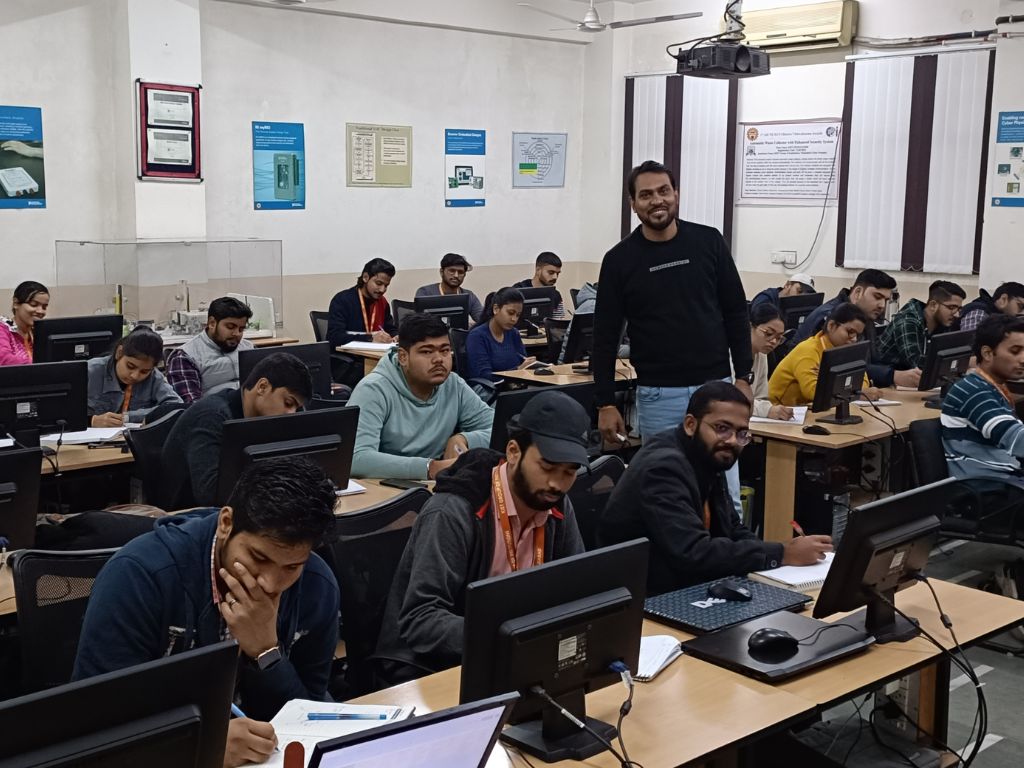
At PinE Training Academy, we focused project based learning on following
- ASIC Design & Full Custom Layout
- Physical Design
- Design & Verification
- Design for Testability
ASIC DESIGN- stands for Application-Specific Integrated Circuit. It is an integrated circuit (IC) customized for a specific use, rather than intended for general-purpose use. ASIC design is the process of designing and developing these customized ICs. This process involves creating a circuit design, verifying that the design meets the specifications, and then manufacturing the IC. ASICs are used in a wide range of applications, including telecommunications, data storage, and consumer electronics. Because they are customized for a specific use, ASICs can be more efficient and cost-effective than general-purpose ICs, such as microprocessors.
What is the full Custom layout?
The full custom layout is a method of designing integrated circuits (ICs) in which the layout of each individual component, such as transistors and interconnects, is done by hand. This allows for a higher degree of control and optimization of the circuit layout, resulting in improved performance and lower power consumption. This method is in contrast to standard-cell or semi-custom layout, in which pre-designed “standard cells” are used to create the layout, providing less control and flexibility. The full custom layout is more time-consuming and expensive than other methods, but it is often used for high-performance, low-power applications such as microprocessors and memory chips.
What are the different career domains in ASIC Design & Full Custom Layout?
- ASIC Design
- Analog Circuit Design
- Analog & Mixed Signal Verification
- Full Custom Layout
- Standard Cell
- Analog Layout
- IO Layout
- Memory Layout
- CAD Engineer
-
- SKILL Automation
Who can join?
Pursuing & Pass out B.Tech\ M.Tech \ M.Sc in Electronics & Electricals Aspirants
Why join?
If Interest in Advanced Analog Design
How PinE can help you in developing interest?
Through Foundation Program
How PinE can help you in making a career?
- Through Pursuing Placement Program
- Through Fresher Pass out Placement Program
- Through Working Professional Training Program
When to join?
- Pursuing Placement Program:-Pursuing 4th year B.Tech/2nd Year M.Tech & M.Sc
- Fresher & Pass out with gap Placement Program
- Working Professional Placement Program
Starting salary of Trained fresher in Analog Profile?
- Multinational Product & Service Company : 15L+ to 16L+ Per Annum
- Indian Product and Service Company: 8L+ to 10L+ Per Annum
Starting salary of Trained fresher in Layout Profile?
- Multinational Product & Service Company: 12L+ to 14L+ Per Annum
- Indian Product and Service Company: 6L+ to 18L+ Per Annum
Companies working in India for Analog and Layout Profile?
-
- MNC: Texas Instrument, Samsung, Intel, Western Digital, OnSemi, Sandisk, NXP, ST Microelectronics, AMD, ADI, Qualcomm, and Many More
- Indian: Vervesemi Microelectronics, Signal ChipYoctozant, Aura Semiconductor, ETEROS TECHNOLOGIES, Einfochip, Signoff Semiconductor, Cientra, Cerium System, HCL, Wipro, Tata ELXI, & Many More
- Selection Criteria
- Throughout 70%
- Written Test & PI
- Trained Freshers from Tier 2 and Tier 3 colleges can join product companies direct.
- No, they cannot join directly. They can be part of the companies through contract, Intern, or Service based Companies.
- How PinE Initiative will support the aspirants looking for Career in VLSI
- Career First Pay Later After the Placement in 12-Month Installment
Physical design in VLSI (Very-Large-Scale Integration) is the process of taking the logical design of an integrated circuit (IC) and converting it into a physical layout that can be manufactured. It includes the following steps:
- Partitioning: The IC is divided into smaller blocks, called cells, which can be designed and optimized independently.
- Placement: The cells are positioned on the IC to optimize performance, power consumption, and manufacturing constraints.
- Routing: Interconnections between cells are created, ensuring that all connections are made correctly and without crossing or overlapping.
- Clock tree synthesis: The clock network is designed and optimized to minimize clock skew and maximize performance.
- Power grid synthesis: A power grid is designed to ensure that all the cells in the IC receive the correct voltage and current.
- Timing closure: The IC is verified to ensure that it meets the timing requirements for each cell and for the overall circuit.
- DRC/LVS: Design Rule Check (DRC) and Layout vs Schematic (LVS) are run to ensure the physical design matches the logical design and that it meets all manufacturing constraints.
- Extraction: The parasitic parameters of the layout are extracted and used in the final timing analysis.
- Tapeout: Final GDSII (GDSII is a format used to transfer layout data between different tools in the IC design flow) or another format is generated and sent to the foundry for fabrication.
Physical design is a complex and time-consuming process that requires a high level of skill and expertise. It is a critical step in the IC design process, as it determines the performance, power consumption, and manufacturability of the final IC.
What are the different career domains in Physical Design?
- STA (Static Timing Analysis ) Engineer
- Synthesis Engineer
- PNR Engineer
- PD Automation Engineer
Who can join?
Pursuing & Pass out B.Tech\ M.Tech \ M.Sc in Electronics & Electricals Aspirants
Why to join?
If Interest in basic Analog and Digital
How PinE can help you in developing interest?
Through Foundation Program
How PinE can help you in making a career?
- Through Pursuing Placement Program
- Through Fresher Pass out Placement Program
- Through Working Professional Training Program
When to join?
- Pursuing Placement Program:-Pursuing 4th year B.Tech/2nd Year M.Tech & M.Sc
- Fresher & Pass out with gap Placement Program
- Working Professional Placement Program
Starting salary of Trained fresher in Physical Design Profile?
- Multinational Product & Service Company : 12L+ to 16L+ Per Annum
- Indian Product and Service Company: 4L+ to 6L+ Per Annum
Companies working in India for Physical Design Profiles?
- MNC:- Nvidia, Analog Devices, Cypress Semiconductor, Mediatek, Micron, Broadcom, Google, Amazon, Meta, Oculus, and Many More
- Indian: Synapse, UST Global, Alten Calsoft, Graphene Semiconductor, Diggicomm, Insemi Technology, Moschip, Smart Soc, Adepts chips Many More
Selection Criteria?
- Throughout 70%
- Written Test & PI
Trained Freshers from Tier 2 and Tier 3 colleges can join product companies direct.
No, they cannot join directly. They can be part of the companies through contract, Intern, or Service based Companies.
How PinE Initiative will support the aspirants looking for Career in VLSI?
Career First Pay Later After the Placement in 12-Month Installment
Verification in VLSI (Very-large-scale integration) design refers to the process of ensuring that a digital circuit, such as an integrated circuit or a field-programmable gate array, meets its design specifications and works as intended. This is typically done through a combination of simulation, formal verification, and testing. Simulation involves using computer software to model the behavior of the circuit and check for errors, while formal verification uses mathematical methods to prove that the circuit meets its specifications. Testing involves physically testing the circuit on a test bench or in a laboratory environment. The goal of verification is to identify and correct errors before the circuit is manufactured, in order to reduce the likelihood of costly defects.
What are the different career domains in Verification?
- RTL Design Engineer
- Verification Engineer
- Automation Engineer
Who can join?
Pursuing & Pass out B.Tech\ M.Tech \ M.Sc in Electronics & Electricals Aspirants.
Why join?
If Interest in C and C++ Programming
How PinE can help you in developing interest?
Through Foundation Program
How PinE can help you in making a career?
- Through Pursuing Placement Program
- Through Fresher Pass out Placement Program
- Through Working Professional Training Program
When to join?
- Pursuing Placement Program:-Pursuing 4th year B.Tech/2nd Year M.Tech & M.Sc
- Fresher & Pass out with gap Placement Program
- Working Professional Placement Program
Starting salary of Trained fresher in Design and Verification Profile?
- Multinational Product & Service Company : 12L+ to 14L+ Per Annum
- Indian Product and Service Company: 5L+ to 7L+ Per Annum
Companies working in India for Design and Verification Profiles?
- MNC:- Cisco, Juniper, Ciena, Synopsys, Cadence, Mentor Graphics, Nordic Semiconductor, Microchip, Marvel Technology, Silicon labs, and Many More
- Indian: True chip, Perfect VIP, Smart Soc, Ensilica, Spicaworks, Skandys, Bitsilica, laksh Semiconductor, Sibridge Technologies, Excel VLSI, and many More
Selection Criteria?
- Throughout 70%
- Written Test & PI
Trained Freshers from Tier 2 and Tier 3 colleges can join product companies direct.
No, they cannot join directly. They can be part of the companies through contract, Intern, or Service based Companies.
How PinE Initiative will support the aspirants looking for Career in VLSI ?
Career First Pay Later After the Placement in 12-Month Installment
DFT stands for Design for Testability, it is a set of techniques and methodologies used in VLSI (Very-large-scale integration) design to make a digital circuit more testable. The goal of DFT is to ensure that a circuit can be thoroughly tested to detect any defects and ensure that it works as intended. This is done by adding additional hardware or modifying the design of the circuit to make it more testable.
- Some common DFT techniques include:
- scan insertion: adding scan chains to the circuit to allow for sequential testing of the internal nodes
- built-in self-test (BIST): adding on-chip test circuitry to the circuit to allow for automatic testing
- at-speed testing: running tests at the maximum operating frequency of the circuit to detect timing-related defects
- boundary scan: adding additional test points to the circuit to allow for testing of the external connections
- The DFT process is considered as an important step in the VLSI design flow and it is used to increase the reliability and reduce the development time and cost of the design
What are the different career domain in DFT?
- DFT Engineer
- DFT Automation Engineer
Who can join?
Pursuing & Pass out B.Tech\ M.Tech \ M.Sc in Electronics & Electricals Aspirants
Why to join?
If Interest in Digital
How PinE can help you in developing interest?
Through Foundation Program.
How PinE can help you in making career?
- Through Pursuing Placement Program
- Through Fresher Pass out Placement Program
- Through Working Professional Training Program
When to join?
- Pursuing Placement Program:-Pursuing 4th year B.Tech/2nd Year M.Tech & M.Sc
- Fresher & Pass out with gap Placement Program
- Working Professional Placement Program
Starting salary of Trained fresher in DFT?
- Multinational Product & Service Company : 12L+ to 14L+ Per Annum
- Indian Product and Service Company: 5L+ to 6L+ Per Annum
Companies working in India for DFT Profile?
- MNC:- All chip manufacturing companies, Advanced Microdevices, Arrow Electronics, and Many More
- Indian: Invecas, Cyient, Aisemicon, Tessolve, Ignitarium Semiconductor, Blackpepper Technologies, Adroitec Systems, Leadsoc, Apex Semi, Alphawave Semi, and many More
Selection Criteria?
- Throughout 70%
- Written Test & PI
Trained Freshers from Tier 2 and Tier 3 colleges can join product companies direct
No, they cannot join directly. They can be part of the companies through contract, Intern, or Service based Companies.
How PinE Initiative will support the aspirants looking for Career in VLSI?
Career First Pay Later After the Placement in 12 Month Installment.
Embedded
What is Hardware Design Hardware design is the process of creating plans for the physical components of a system or machine? This includes designing the individual components, such as circuit boards, chips, power supplies, and other elements, as well as the overall system architecture. The goal is to create a functional, reliable, and cost-effective product. Hardware design also involves creating detailed drawings and specifications of the components, as well as planning their assembly. This includes the selection of materials and components, the design of the printed circuit boards, and the testing of the designs. Hardware design is a critical process in the development of any technology product since it is the foundation of the product’s success. Properly designed hardware will provide reliable performance, reduce the cost of production, and ensure the product meets customer expectations. Hardware design is often carried out by engineers, who have an understanding of electronics and have experience in the design and production of hardware. Good hardware design requires knowledge of the specific application and a thorough understanding of the available components and materials. The design process should also incorporate user feedback and testing to ensure the final product is as functional and reliable as possible. Good hardware design will often result in a product that performs better, is cheaper to produce, and is more reliable and durable than if the design had been rushed or done without proper consideration.
The domain of hardware design involves the development of physical electronic components and systems. This includes designing and testing of circuit boards, component selection, circuit simulation, and the integration of physical components into larger systems. Hardware design also covers the development of embedded systems, such as programmable logic devices, microcontrollers, and digital signal processors. Additionally, hardware design includes the development of software to interact with the hardware components, such as device drivers, operating systems, and other software tools.
At PinE Training Academy, we focused project based learning on following
- FPGA System Design
- Embedded System Design
- PCB Design
FPGA stands for Field Programmable Gate Array. It is an integrated circuit (IC) that can be programmed to perform a variety of tasks. FPGAs contain programmable logic components called “logic blocks,” and a hierarchy of reconfigurable interconnects that allow the blocks to be “wired together” almost like many logic gates that can be reconfigured to desired application or functionality requirements. FPGAs are used in a wide variety of applications, from cell phones and computers to medical devices and industrial automation. The major advantages of FPGAs are their flexibility, low power consumption, and fast prototyping. FPGAs can be used to implement a wide variety of digital and analog functions, from basic logic gates to complex processors and other systems. They are also cheaper than other types of integrated circuits and can be quickly reprogrammed for different functions, making them ideal for prototyping or testing. FPGAs are also used in embedded systems and digital signal processing (DSP) applications, where their programmability can be used to adapt them to the changing requirements of the system. FPGAs are also used in high-performance computing, where their speed and flexibility can be used to solve complex problems quickly. They are also used in networking and storage, where their low power consumption and high data rates can be used to reduce system costs. FPGAs are an important part of the modern digital world and are likely to become increasingly popular in the future.
Who can join?
Pursuing & Pass out B.Tech\ M.Tech \ M.Sc in Electronics & Electricals Aspirants.
Why to join?
If Interest in Hardware Programming.
How PinE can help you in developing interest?
Through Foundation Program.
How PinE can help you in making career?
- Through Pursuing Placement Program
- Through Fresher Pass out Placement Program
- Through Working Professional Training Program
When to join?
- Pursuing Placement Program:-Pursuing 4th year B.Tech/2nd Year M.Tech & M.Sc
- Fresher & Pass out with gap Placement Program
- Working Professional Placement Program
Starting salary of Trained fresher in FPGA Design.
- Multinational Product & Service Company : 10L+ to 12L+ Per Annum
- Indian Product and Service Company: 4L+ to 5L+ Per Annum
Companies working in India for FPGA Design
- MNC:- Cisco, Ciena, Altera (now Intel), Lattice Semiconductor, Xilinx (now AMD), Achronix, Microsemi, Mathwork, Boeing, and Many More
- Indian: Astra, Data Patterns, Lekha wireless, Megh Computing, Saankhya Labs, Mistral Solutions, Bit Mapper, Aujus Technology, Logic-Fruit, Anayatech, and many more
- Selection Criteria +
- Throughout 70%
- Written Test & PI
- Trained Freshers from Tier 2 and Tier 3 colleges can join product companies direct+
- No, they cannot join directly. They can be part of the companies through contract, Intern, or Service based Companies.
- How PinE Initiative will support the aspirants looking for Career in VLSI +
- Career First Pay Later After the Placement in 12-Month Installment
Embedded system is a computer system that has a specific purpose and dedicated hardware. It is not a general-purpose computer, like a desktop or laptop. Embedded systems are found in a variety of devices, including cars, medical devices, digital cameras, and home appliances. Embedded systems are designed to do a specific task, rather than be a general-purpose computer that can be used for a variety of tasks. For example, a desktop or laptop can be used for word processing, browsing the internet, and playing games. An embedded system, such as a digital camera, is designed to take pictures. Embedded systems are often powered by a dedicated processor and have a limited amount of memory. They typically do not have a keyboard, mouse, or display. Instead, they are controlled by a set of commands that are input through a special port. Embedded systems are often used in devices where size and power consumption are important factors. For example, a digital camera needs to be small and light so that it can be easily carried around. A desktop or laptop is not as constrained in terms of size and power consumption. Embedded systems are often more reliable and stable than general-purpose computers. This is because they are specifically designed for a single task and are not as complex. Embedded systems are usually more expensive than general-purpose computers. Embedded systems are often more difficult to program than general-purpose computers. This is because they often have a limited amount of memory and processing power.
Who can join?
Pursuing & Pass out B.Tech\ M.Tech \ M.Sc in Electronics & Electricals Aspirants.
Why to join?
If Interest in Hardware Programming.
How PinE can help you in developing interest?
Through Foundation Program.
How PinE can help you in making career?
- Through Pursuing Placement Program
- Through Fresher Pass out Placement Program
- Through Working Professional Training Program
When to join?
- Pursuing Placement Program:-Pursuing 4th year B.Tech/2nd Year M.Tech & M.Sc
- Fresher & Pass out with gap Placement Program
- Working Professional Placement Program
Starting salary of Trained fresher in Hardware Programming.
- Multinational Product & Service Company : 10L+ to 12L+ Per Annum
- Indian Product and Service Company : 4L+ to 5L+ Per Annum
Companies working in India for Hardware Programming.
- MNC:- Delphi Automotive, Visteon Corporation, John Deere, Robert Bosch, Caterpillar, Ashoka Motors, Tata Motors, L & T, Honeywell and KPIT Cummins and Many More
- Indian: Ittiam System, Mphasis, Symphony,Sonata, Dexcel, Robosoft, Neuphony,Semtronics Microsystems, Rhydo Technologies,Captronic Systems and many More
Selection Criteria
- Throughout 60%
- Written Test & PI
Trained Freshers from Tier 2 and Tier 3 colleges can join product companies direct.
No, they cannot join directly. They can be part of the companies through contract , Intern or Service based Companies.
How PinE Initiative will support the aspirants looking for Career in VLSI?
Career First Pay Later After the Placement in 12 Month Installment.
PCBs are made up of a number of different layers. The layers are typically divided into four categories: top, bottom, middle, and inner. The top and bottom layers are the outermost layers of the PCB. The middle layer is the layer in the middle of the PCB. The inner layer is the layer closest to the components on the board.
Who can join?
Pursuing & Pass out B.Tech\ M.Tech \ M.Sc in Electronics & Electricals Aspirants.
Why to join?
If Interest in Digital.
How PinE can help you in developing interest?
Through Foundation Program.
How PinE can help you in making career?
- Through Pursuing Placement Program
- Through Fresher Pass out Placement Program
- Through Working Professional Training Program
When to join?
- Pursuing Placement Program:-Pursuing 4th year B.Tech/2nd Year M.Tech & M.Sc
- Fresher & Pass out with gap Placement Program
- Working Professional Placement Program
Starting salary of Trained fresher in PCB.
- Multinational Product & Service Company : 18L+ to 20L+ Per Annum
- Indian Product and Service Company: 7L+ to 8L+ Per Annum
Companies working in India for PCB Profile
- MNC:- All chip manufacturing companies and Product Companies have a PCB Design team
- Indian: Absolute Advance, Acme Inspire, Camtech PCB, CPV Technologies, ELDASS Circuits, Elite Technologies,Flextronics Pvt ,Glonix electronics,Green Circuits ,Hypen Electronics and many more
Selection Criteria?
- Throughout 60%
- Written Test & PI
Trained Freshers from Tier 2 and Tier 3 colleges can join product companies direct.
No, they cannot join directly. They can be part of the companies through contract, Intern, or Service based Companies.
How PinE Initiative will support the aspirants looking for Career in VLSI?
Career First Pay Later After the Placement in 12 Month Installment
